
06 May 100% inline control during laser drilling of microvias
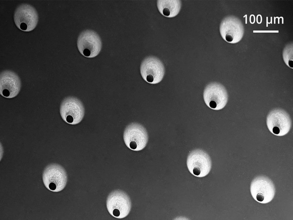
In the production of modern printed circuit boards with high conductor and component density, the connections between the layers are drilled using lasers. The microvias have diameters of less than 200 µm. The drilling process must be fast, cost-effective, flexible and, above all, precise, as the holes form the electrical contacts between the metal layers of the PCB after metallisation. Insulation material must therefore be completely removed during the drilling process in order to achieve good contacting, which determines the function and durability of the electronics. Today, the quality inspection of microvias is carried out downstream, sometimes using destructive methods such as cross-sectioning or electrical function testing – and often only on a random basis, which is not sufficient for safety-critical applications.
Inline testing and process control
In the ‘Hilam’ research project (highly dynamic inline control of laser drilling of microvias), researchers at the Fraunhofer Institute for Physical Measurement Techniques IPM are working with 3D-Micromac and Berlin-based Andus Elektronik to develop an optical process that can be used to check the quality of microvia drill holes using ultrashort pulse lasers (USP) during the process and automatically control the drilling process. USP lasers are increasingly being used for the structuring of printed circuit boards, as they can drill holes with very small diameters in challenging materials. However, USP lasers are not material-selective and therefore require control, as the thickness and homogeneity of the insulation layers fluctuate.
LIBS – spatially resolved drilling control in real time
According to the researchers, they use laser-induced breakdown spectroscopy (LIBS) to analyse and control the ablation process with pulse resolution – selectively and spatially resolved within a hole. The LIBS sensor is integrated into the system coaxially to the ablation laser and records the material-specific plasma emission that occurs during material ablation. The spectrum can be used to determine which material was ablated. If the plasma spectrum shows copper, this means that the insulation layer has been sufficiently ablated at the corresponding point. In this case, the control algorithm decides that the laser is aligned to the next position within the drill hole. This should enable one hundred per cent inline quality control.
Hilam project
The project is funded by the German Federal Ministry of Education and Research (BMBF) as part of the ‘Photonics for the digitally networked world – rapid optical control of dynamic processes’ funding programme. The project partners are 3D-Micromac (project coordination), Andus Elektronik and the Fraunhofer Institute for Physical Measurement Techniques IPM.
Source: www.ipm.fraunhofer.de
Image: 3d-micromac.de

