
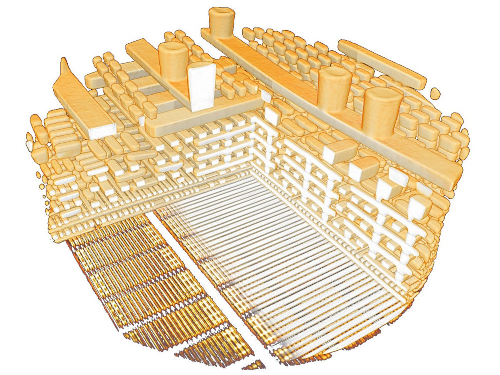
13 Aug A look inside a computer chip with 4 nanometer precision
High-resolution three-dimensional images of a computer chip were created by researchers from Switzerland and USA using a non-destructive method based on X-ray tomography. The collaboration has made it possible for the first time to take images of ultra-modern computer chips with a resolution of 4 nanometers – a new world record, according to the partners from the Paul Scherrer Institute PSI, EPFL, ETH Zurich and the University of Southern California. Instead of relying on lenses that are currently impossible to manufacture for imaging in this size range, the researchers used a computer process that combines many individual images into one high-resolution image. For their experiments, the researchers used X-ray light in the Swiss Light Source SLS at PSI.
Between X-ray tomography and electron microscopy
Today, nanometer-sized interconnects are etched into silicon blanks in clean rooms using highly automated optical systems. Layer after layer is applied and removed until the finished chip can be cut out and installed. What already is an elaborate and complicated production process proves to be just as difficult when it comes to characterizing and imaging the structures produced.
Scanning electron microscopes allow a resolution of a few nanometers and are therefore well suited to imaging the tiny transistors and metal connections that make up the circuits. However, they can only produce two-dimensional images of the surface. “The electrons don’t penetrate deep enough into the material,” explains Mirko Holler, physicist at the SLS. “In order to reconstruct three-dimensional images, the chip has to be examined layer by layer and each layer has to be removed individually in the nanometer range – a very complex and delicate process, and the chip is destroyed in the process.”
Three-dimensional and non-destructive images, on the other hand, can be produced using X-ray tomography, as X-rays can penetrate materials much better. The sample is rotated and X-rays transmit through it from different angles. Depending on the structure of the sample, the radiation is absorbed and scattered differently. A detector registers the emerging light and an algorithm reconstructs the finished 3D image from it. But: “This is where we have the problem with resolution,” explains Mirko Holler. “There are currently no X-ray lenses that can focus this radiation for imaging such tiny structures.”
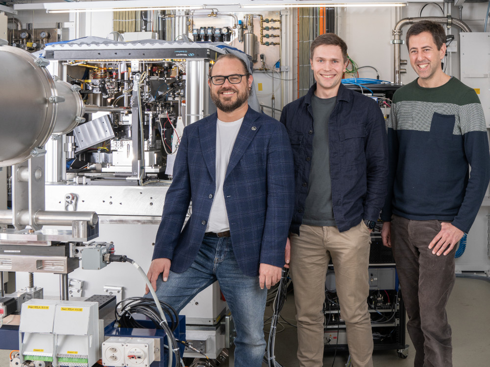
Manuel Guizar-Sicairos, Tomas Aidukas and Mirko Holler (from left) in front of their measurement setup in the Swiss Light Source SLS at PSI. The researchers achieved a new world record with the X-ray light generated here. Image: Mahir Dzambegovic / Paul Scherrer Institut PSI
Not bundled but shifted
The solution is called ptychography. In this method, the X-ray beam is not focused in the nanometer range, but the sample is shifted in the nanometer range. “Our sample is moved in such a way that the beam can follow a precisely defined grid – similar to a sieve,” explains Holler. “A scattering image is then recorded at each grid point.” The distance between the individual grid points is smaller than the diameter of the beam so that the imaged areas overlap. This allows enough information to be recorded to reconstruct the image of the sample in high resolution using an algorithm. The reconstruction process is a kind of virtual lens.
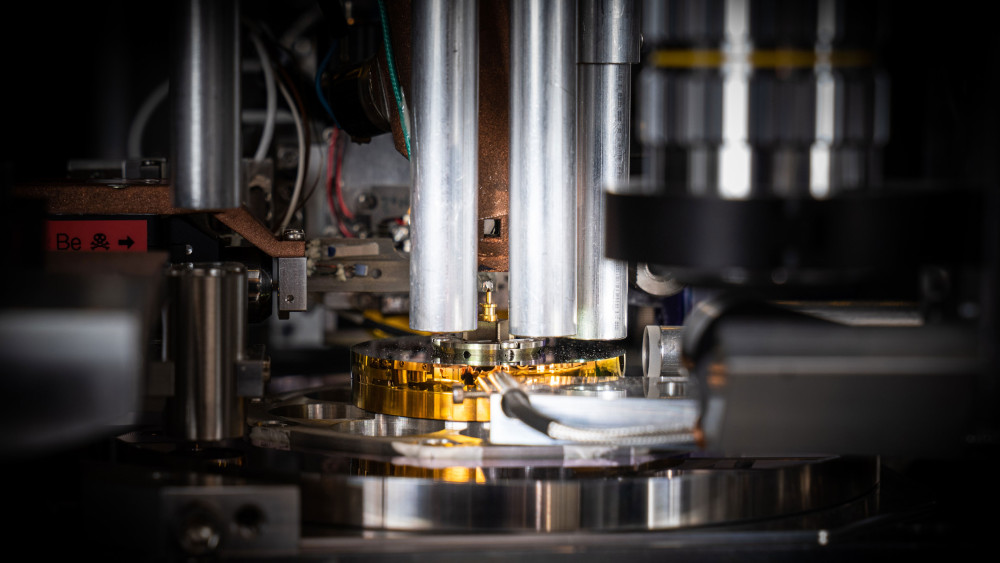
The sample, a cylindrical section of a commercially available computer chip, is held by the gold-coloured needle in the centre of the image. The sample was cut out of the chip with a focussed ion beam and placed on a pin. Image: Mahir Dzambegovic / Paul Scherrer Institut PSI
New approaches for the highest resolutions
The partners achieved the new resolution record through shorter exposure times and a new algorithm. When they reduced the exposure time, the diffraction images were sharper. This led to the conclusion that the X-ray beam may not hit the sample evenly, but instead performs a tiny movement – it wobbles. Although they now had sharp images, the short exposure time meant that they contained too little information to reconstruct the entire computer chip.
To solve the problem, the researchers supplemented their setup with a faster detector, which was also developed at PSI. This allowed them to take many images per grid point with a short exposure time. “An enormous mountain of data,” adds Aidukas, the physicist involved. If you add up the individual images and superimpose them, you get the original, blurred image again – equivalent to the long exposure time.
“Imagine the X-ray beam as a point on the sample,” explains Aidukas. “I now take many individual images at this point.” As the beam wobbles, each image will change slightly. “In some images, the position of the beam matches, in others it deviates. Based on these changes, we can track the actual position of the beam, which is caused by the unknown vibrations.” The next step is to reduce the amount of data. “Our algorithm compares the beam positions of the individual images,” Aikdukas continues. “If the positions match, they are placed in the same group and summarized there.” This grouping increases the information content of the low-exposure images. In this way, the researchers are able to reconstruct a sharp result with a high light content from the short-exposure flood of images.
Further fields of application
According to the researchers, the novel ptychography process is a fundamental approach that is not limited to computer chips, but can also be used for other samples, for example in the materials or life sciences.
Originalpublikation:
[High-performance 4 nm resolution X-ray tomography using burst ptychography, Tomas Aidukas, Nicholas W. Phillips, Ana Diaz, Emiliya Poghosyan, Elisabeth Müller, A.F.J. Levi, Gabriel Aeppli, Manuel Guizar-Sicairos, Mirko Holler, Nature, 31.07.2024, DOI: 10.1038/s41586-024-07615-6]
Link to a YouTube video about the microscopy method
Source: www.psi.ch
Image: Tomas Aidukas / PSI

