04 Jul Silicon-based photodiodes for cheaper IR-sensors
In the visible range, almost all photodiodes today are made of silicon, as this material can be produced cost-effective as a standard in the semiconductor industry. However, in the near infrared range, silicon-based photodiodes have so far reached their limits due to their low sensitivity. For this reason, materials such as indium gallium arsenide (InGaAs) are used in this field. Though, this material requires its own manufacturing processes, which are not compatible with silicon semiconductor technology and are therefore expensive. In addition, harmful heavy metals such as arsenic are used in the manufacturing process.
As part of the new research project ‘Messi – Research into thin metal layers on structured silicon substrates’, researchers at the Fraunhofer Institute for Photonic Microsystems IPMS are now developing for the first time sensitive, silicon-based photodiodes that can be produced cost-effectively.
Silicon restructured
“The innovation is based on the implementation of a new structure in our photodiode,” explains project coordinator Michael Müller from Fraunhofer IPMS. “Instead of the usual planar device topography, we use new pyramidal and ring structures that function like a light collecting basin. Using a very thin metal layer in the Schottky junction, we increase the internal quantum efficiency – that means the number of charge carriers generated by light in the semiconductor.”
According to the researchers, these two innovations should significantly increase sensitivity and enable applications in the near infrared with silicon photodiodes for the first time. The new approach should not only offer economic advantages by utilizing established silicon semiconductor technologies, but also ecological advantages, as the use of heavy metals can be avoided. This makes a decisive contribution to sustainability in the semiconductor industry.
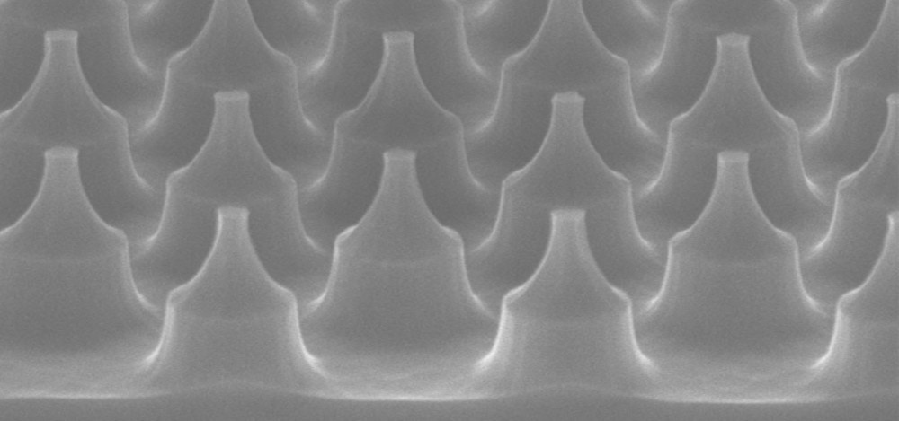
Scanning electron microscope image of the cylindrical pyramidal structures of the silicon photodiodes.
Image: Fraunhofer IPMS
Applications from lidar to spectroscopy
According to the researchers, silicon photodiodes could enable a range of new applications in the near-infrared range in the future, especially in price-sensitive volume markets. One example is autonomous driving, which requires new lidar sensors and fog cameras for effective environmental monitoring. This is particularly important when visibility is obstructed by smoke or fog and cameras in the visible range fail. There are also numerous applications in chemical and medical imaging as well as spectroscopy. Specifically, hyperspectral imaging in the near infrared is used in process measurement technology in the pharmaceutical and chemical industries to detect and analyze organic materials and material mixtures.
The Federal Ministry of Education and Research in Germany (BMBF) funds the Messi project with 566,000 euros for a period of three years.
Source and image: www.ipms.fraunhofer.de

