03 Jun From small to large-scale production: glass substrates for semiconductors
The semiconductor industry is shifting from organic and silicon substrates to glass. According to players in the semiconductor industry, glass substrates are set to become the new market standard. Advanced packaging and heterogeneous integration are used to produce chips using various advanced manufacturing processes, which are then integrated into a semiconductor package. An important component here is glass as a substrate material. With Laser Induced Deep Etching (LIDE), LPKF wants to pave the way for the transition to this new era from small series products to large series production.
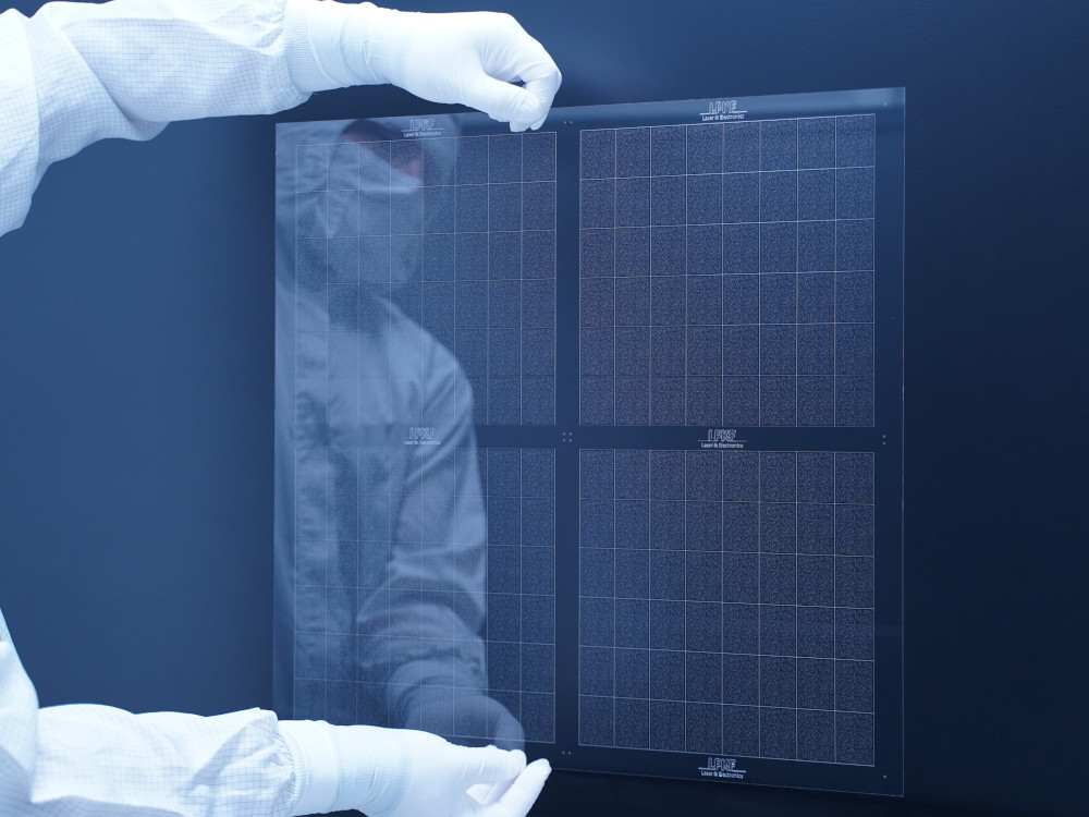
Over the past 10 years, LPKF says it has developed its industrial processes for glass production with high quality standards and a focus on throughput in order to fulfil industrial requirements. According to the company, their own LIDE process is well established. Glass substrates from 100 μm to 1.1 mm can be processed quickly, precisely and without damage such as microcracks, emphasizes LPKF. According to CEO Dr Klaus Fiedler LPKF should now be able to provide production capacities for large-scale production. ‘Our technology has reached an outstanding level of maturity to fulfil the requirements of the semiconductor industry. For this reason, we have increased our production capacities in 2024 to meet increasing customer demand.’ The company also says it supports customers in the introduction of glass cores for advanced packaging applications by integrating the technology into customers’ manufacturing processes or offering manufacturing services through its Vitrion division.
Link to a YouTube video on the LIDE process
Information page on LIDE from LPKF
Source and image: www.lpkf.com

