14 Jun STMicroelectronics and Metalenz cooperate in the industrialisation of metasurface optics
Semiconductor manufacturer STMicroelectronics has signed a development and licensing agreement with Metalenz. As a result, ST will develop manufacturing processes for the company’s meta-optics technology: ST intends to integrate the technology into its process for manufacturing diffractive optics, which is located at the company’s 300 mm wafer fab in Crolles, France. ST’s position in the rapidly expanding NIR sensor market is expected to be advantageous, where the manufacturer sees itself at the forefront of the market for ToF (time-of-flight) proximity and distance sensors, of which it says it has already shipped more than a billion units.
According to ST and Metalenz, the near infrared is initially the most important application area for metasurface optics. NIR light is used in all 3D sensor functions, such as face recognition, autofocus support, mini-lidar and depth maps for AR/VR systems, which will gradually become standard equipment in smartphones. In addition to upcoming smartphone generations, healthcare and automotive applications are also mentioned as fields of application.
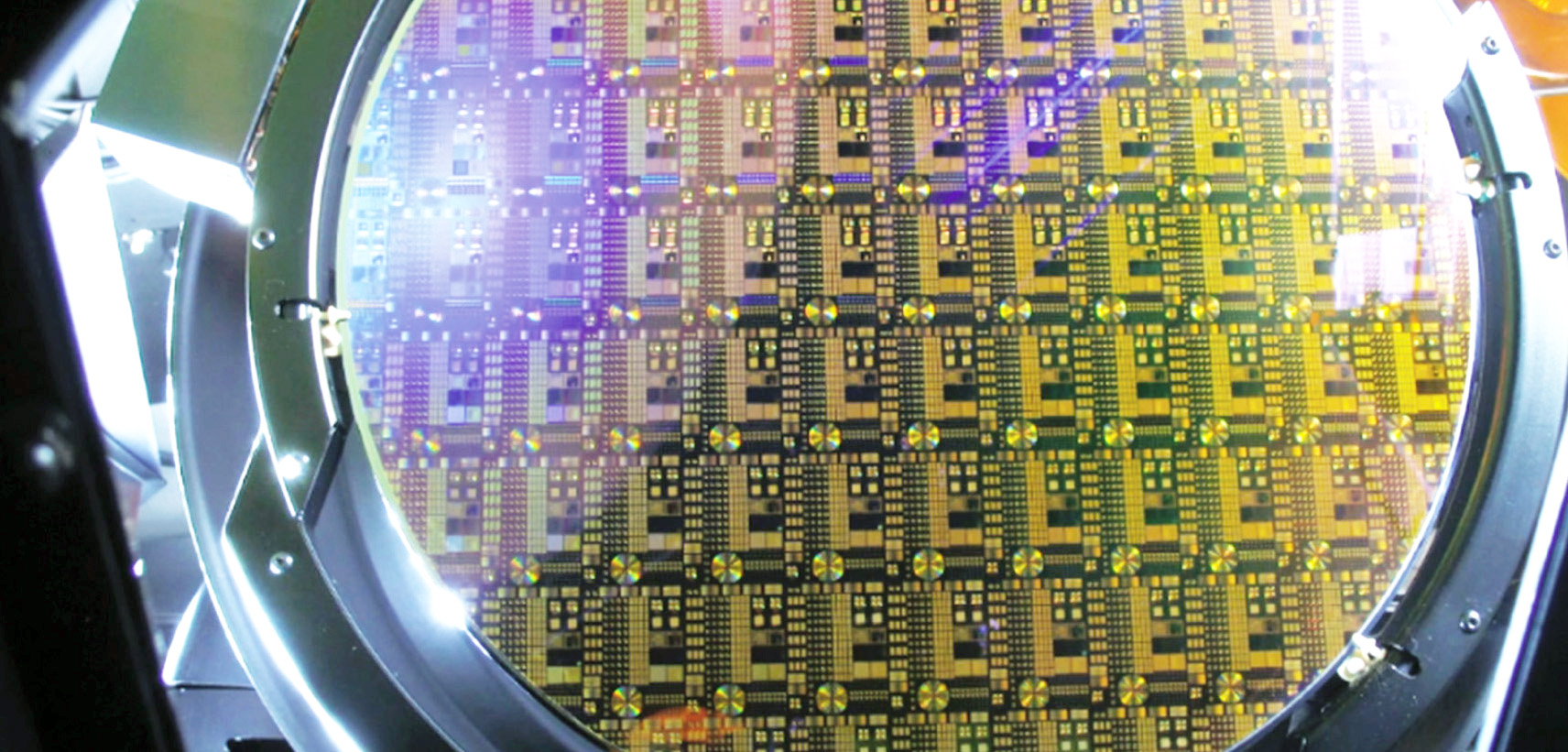
ST now wants to use advanced lithography masks to produce tunable diffractive wavefront layers on a meta-surface in a semiconductor wafer fab. Like silicon ICs, the flat metasurface lenses are manufactured – using the same production technology – in a clean room designed for semiconductor production.
Unlike conventional lenses, metasurface lenses contain nanostructures that can be used to realise several complex optical functions in a single layer, for which an optical system consisting of several refractive lenses is traditionally required. On the one hand, this reduces the size of the individual lens elements; on the other hand, the number of necessary components is reduced, so that smaller lenses can be constructed and the complexity of the structure decreases.
Source and image: https://www.st.com


